Ground Gain
K9 Analysis introduces the concept of Ground
Gain. The Ground Gain is simply the voltage gain from the ground node to the
circuit output. Legacy Analysis ignores ground gain. The ground node has a potential
of zero volts and regardless of the gain, can not affect the output voltage.
Why do I need to consider ground?
Experienced analog designers have discovered
that the ground voltage is never equal to zero volts. All systems have noise on
the ground node, which can corrupt the output signal. Minimizing the
ground voltage or the ground gain can reduce output noise.
Let’s examine ground in more detail. Consider
the figure below:
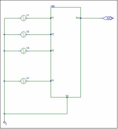
The figure is intended to be the simulation
schematic for any circuit. The circuit is included in block HB1. Only the
interfaces to HB1 are shown in the figure. Ports P1 to Pn
receive ideal voltage source inputs. Port P0 is the ground reference for HB1.
Port Pout is the output node of HB1. Pout can be any node in HB1.
Ground
Ground is simply a reference node. Spice
reserves the node name "0" for ground. In theory, ground can be any
node in your circuit. In practice you need to pick the ground node carefully.
If you pick a node that is not common to a lot of signals your circuit
equations can become very complex.
Consider the following analogy:
In the early days astronomers described the
movement of the planets with Earth as the reference point. This created some
rather complex patterns. In the Middle Ages
astronomers discovered that if you used the Sun as a reference, the planet
movement could be described with simple ellipses.
The VSA analysis procedure used by K9 Analysis does not allow floating voltage sources. A
good ground node choice for VSA is the common point of the input voltage
sources.
Ground
Noise
Experienced analog designers always try to
reduce the amount of noise induced into the ground lead connections. (I hate
solving noise problems.) Even with large ground planes, there is always some
signal on the ground lead. This noise is shown in the figure below as V0.

V0 is an ideal voltage source that represents
the noise voltage on the ground lead. If the noise voltage has source
impedance, it should be included in HB1. The ground noise is thus simply
another input to HB1. Like any input it has a gain from the voltage source
input to the output. The voltage gain from V0 to V(out)
is the ground gain. Since Spice uses "0" for the ground node name, K9
Analysis uses V0 for the ground noise voltage and G0 for the ground gain.
Application
It should be intuitively obvious that there
are two ways to reduce the effect of output ground noise on an output. The
first is to reduce the magnitude of the ground noise voltage. The second is to
reduce the ground gain. Daisy’s Theorem provides an
easy method for calculating Ground Gain.