State Variable Filter
The State Variable Filter
circuit below has a
Whenever you find an interesting circuit, simulate the circuit to verify any claims made in the circuit description. The simulation forces you to provide a complete description. Input sources are often not shown. In this case, an ideal voltage input is assumed. Constructing a simulation schematic may take a little time, but is worse the effort.
The simulation output for a 1KHZ design is shown below.
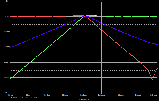
The output is shown on a log-log graph. The Low pass output is red, the band pass blue, and the high pass green. This circuit works.
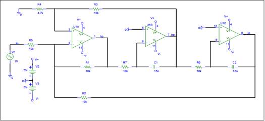
The circuit contains three op-amps. U1A appears to be a summing amplifier with multiple inputs. U1B and U1C are integrators. You can build this circuit using a single LM324 quad op-amp.
This circuit contains multiple feedback loops. The bp and lp outputs feed back to the hp input. Can this circuit be analyzed via Electronic circuit reduction, the bag of tricks approach? I posed the challenge to a colleague. The next day he showed me a simple procedure which reduced the circuit and extracted the output equations. He did use Daisy’s theorem. If you’re skilled at Electronic tricks this is not difficult. For the rest, I recommend K9 analysis.
Construct the Signal Flow Graph
The first step is to add the SFG nodes. Instead of a detailed analysis, the op-amp circuit operation is assumed to be ideal. This allows the op-amp circuits to be modeled as amplifiers. The circuits are a form of General Summing Amplifier. Plato’s Gain Formula applies since all amplifier inputs are voltage controlled nodes.
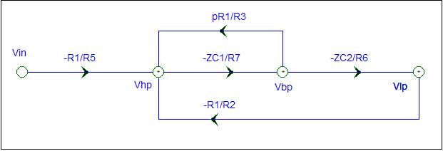
The input node and output nodes have labels. The voltage, at these nodes, will be the SFG nodes.
We skipped the step of converting the components to impedance. The analysis is hence restricted to the above circuit.
Vhp is the output of a summing amplifier. There are two negative gain inputs and a positive gain input.
p = ZP+/ZP- = (4.7k // 10k) / (10k // 10k //10k) = 3.2k/3.33k = 0.96 = ~ 1
The Vhp gains are shown on the SFG below.
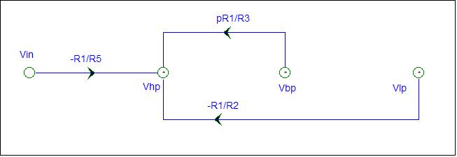
Vpb and Vlp are the output of integrator circuits. No problem, just use the impedance values. The impedance of C1 is ZC1 and the impedance of C2 is ZC2. The integrator gain is –Zf/Zi.
ZC1 = 1/sC1 ZC2 = 1/sC2
The SFG is complete. We need to perform a validity check.
The input Vin has only an outward branch.
Vhp, Vbp, and Vlp are voltage control nodes.
The amplifier gains are of the Zf/Zi form.
Analyze the Signal Flow Graph
The SFH contains two loops.
L1 = -ZC1/R7 * pR1/R3
L2 = -ZC1/R7 * -ZC2/R6 * -R1/R2
∆ = ( 1 – L1 – L2 ) = (1 + ZC1/R7 *pR1/R3 + ZC1/R7 * ZC2/R6 * R1/R2)
The ∆ term contains only positive components, a good sign of stability. The filter outputs are the SFG paths from Vin to an output.
Vhp = (-R1/R5) / ∆ * Vin
Vbp = (R/R5* ZC1/R7) / ∆ * Vin
Vlp = (-R/R5* ZC1/R7 * ZC2/R6) / ∆ * Vin
Each output has only a single path from Vin. Removing the path removes the loops. The numerator ∆ term is thus equal to one.
The easy part of the analysis, obtaining the gain equations, is done. You now need to match the equation with filter equations. Reader exercise.
Modeling the op-amp circuits as a General Summing Amplifier allowed a simple analysis. You need to verify that all amplifier inputs are ideal voltage sources. Any voltage controlled node qualifies.