Signal Flow
The intent of K9 Analysis is to make Analogue Circuit Analysis Dog-Gone-Simple. The most difficult part is to explain circuit operation. How does a circuit work? Electronics has many explanations, too many. Only the circuit knows for sure.
In K9, a circuit is a set of electronic components that has at least one input and at least one output. The circuit operation is described by signal flow from the input to the output. Concentrating on Signal flow rather than Voltage or Current, allows a simple circuit description. This is the philosophy. In practice, Signal Flow descriptions are not unique. On this page Signal Flow is discussed. Since the K9 VSA procedure automatically creates a Signal Flow description, you can skip this page.
The Schematic diagram layout is very important. You want to clearly illustrate the important information. You want to minimize wire crosses and create a pretty picture. A schematic should be a picture suitable for framing and provide an intuitive description of circuit operation. In a schematic a lot of the information is displayed in a subtle manner by the layout, i.e. the placement of components.
For Circuit Analysis, we need to show the information needed for analysis. This includes the component type and electrical value. Other data can be hidden. A simulation schematic contains the information needed to perform a circuit simulation. It can be used for circuit analysis. It’s also a good validity check. If a schematic lacks inputs or attempts to violate a circuit law, the simulator will issues error warnings and refuse to simulate the circuit. A simulation schematic from the schematics page is shown below.
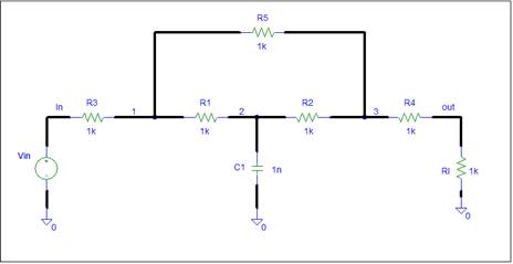
The schematic shows the netlist, the input stimuli, and the output load. The circuit components and nodes are labeled. This is sufficient for analysis. For a clear circuit description we need to make the schematic layout reveal the circuit operation.
Inputs should be on the left and outputs on the right. The circuit input signal travels from left to right across the schematic. This is what circuit do. They take input stimuli and propagate the input signals to the output. In a good schematic, the input to output signals paths should be obvious and only flow from left to right across the schematic.
The left to right signal flow is arbitrary. The circuit does not know what the schematic looks like and simply does not care. The circuit will continue to do its thing. We need to mold the circuit operation description into a standard signal flow template. For clarity, inputs must be on the left and outputs on the right. The Left side of a schematic should contain only inputs. Similarly, the right side should contain only outputs. This is very important. Don’t violate this rule.
How do signals propagate from
input to output? There are many possible descriptions. K9 relates signal flow
to the schematic. Signals can only flow thru circuit components. The schematic
shows what components are present and how they are connected. Signals flow is
via circuit paths. In this case there are two direct signal paths from the
input to the output. The input signal can go thru R3 to node 1,
and thru R1, R2, and R4 to the output. The other path is input thru R3, R5, and
R4 to the output. Paths which go thru a node more than once don’t count.
A Signal Flow Graph (SFG) displays the signals more clearly via a directed graph. There are many ways to create a SFG. The traditional approach is to create the SFG from a set of equations. In this case the signal flow may not match your circuit intuition. The K9 VSA procedure creates the SFG from the circuit schematic. Signal flow is thru circuit components and the SFG layout matches the schematic layout. This creates a good signal flow description if the schematic has a good layout. The VSA SFG for the above circuit is shown below.
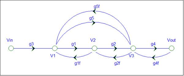
Signal flow is shown via
directed branches. The gain labels were selected to match the resistor label.
Each resistor creates signal flow in two directions. Components can require two
branches. The left to right main signal flow and reverse signal flow denoted by
the f (feedback) in the label.
The reverse signal flow for R3 has a gain of zero. Vin is an ideal voltage source. The circuit can not change the value of this source. To keep things simple, zero gain branches are not shown.
The signal paths have gains.
The gains are shown on the SFG. You don’t need to consider the gains. Brandy will provide the passive circuit gains and Mason will correct the path
gains for circuit interaction. You need to concentrate on the difficult part,
making a clear circuit description.
The schematic should emphasize the main signal flows. The components that create the main signal path are placed horizontally. Components that connect to ground are shown with a vertical orientation. They are not part of the main input to output signal path. The orientation can thus be used to make the input to output signal path more obvious.
If the schematic is an
accurate description of the Signal Paths, the circuit description can be the
schematic or the SFG. You may not have to write a lengthy
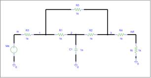
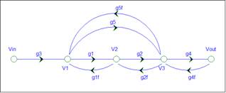
dissertation. The table below shows the schematic and the VSA SFG.
|
Schematic |
VSA SFG |
|
|
|
The schematic and SFG also
shows Feedback paths. A Feedback path is a circular path. Signal flowing from right
to left can create feedback. Passive components allow signals to flow in both
directions and create lots of feedback loops. Active components have signal
flow in only a single direction and are much easier to analyze.
Feedback can also be created by multiple components. The SFG shows a loop from V1 to V2 to V3 and back to V1. This loop shows interaction between R1, R2 and R3. The VSA procedure automatically handles feedback. You don’t have to consider feedback. Just enjoy the art of the loops.
The K9 VSA procedure only
shows some of the signal flow in the SFG. Note that the SFG has no ground node.
There are no SFG branches for vertical components connected to ground. The ground components are included in the Node
impedance and can affect the magnitude of a branch gain, but they do not create
branches in the SFG.
The VSA procedure hides all
ground signal paths. Why? They are not needed to calculate the circuit transfer
function. Only the signal paths for a complete description are shown on a SFG.
A SFG must represent a valid set of circuit equations. Redundancy is not
allowed.
The problem is that there are many different sets of complete descriptions. The SFG can only show one. This is discussed on the SFG page.
The ground signals are
present in the circuit. To see the ground signal path, connect the ground nodes
via wires and remove the ground label.
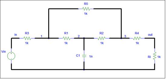
In the above schematic there are multiple signal paths from the input to the output via the old ground node. The paths go thru components that connect to the old ground, in this case the paths go thru C1 and Rl. We should change the orientation to horizontal, if we want to show that these components are part of the main signal flow.
In the VSA procedure, the selection
of the Ground Node will determine which signal paths
are hidden. If you select a different node for ground, you will have a circuit
with a different signal flow description. The circuit behaves the same
since the connections are the same, but the circuit description will be very
different. In the above schematic, if you select node 1 as the
ground node. Both of the previous signal paths will become hidden. The new
signal paths are the previous hidden paths thru C1 and Rl.
Changing the ground node
assignment is an easy way to create a new novel circuit. Just take a special
circuit, connect all ground wires. Remove the ground assignment and pick a new
ground node that is part of the old signal flow. Redraw the circuit to meet
schematic rules. Viola, you have just invented a new novel circuit. Give the
credit to your dog. The circuit is not aware of the schematic change and will function the same.
Why are some signals shown, while others are hidden? Let’s look at signals more closely.
Legal Issues
Electronic circuits must comply with Kirchoff’s circuit laws. If you know all but one of the voltages in a loop, Kirchoff’s Voltage law specifies the remaining voltage. Similarly if you know all but one of the currents flowing into a node, Kirchoff’s Current law specifies the remaining current. K9 introduces a new circuit law in Daisy’s Theorem. The voltage signal gains must add to one. This makes one of the voltage signal gains redundant. In addition to the general laws, there may be special laws that only apply to a specific circuit. Don’t attempt to violate a Law! Real Circuits obey all circuit laws. Compliance is mandatory.
The circuit laws create redundancy. An Electronic analysis procedure needs to remove the redundancy to create an independent set of equations. This is done automatically by the procedure. You don’t have to consider this. Just follow all the rules. Don’t skip any steps. If you choose not to follow an accepted procedure, you need to guarantee that the equations are complete and independent, and check your answers.
The VSA procedure is based on
Nodal Analysis . The
equations are Kirchoff’s Current law applied to circuit nodes. There
is one equation for each circuit node. The variables are the node voltages with
respect to a ground node. The number of node voltages is one less than the
number of nodes. If you want to solve the
equations , you need to eliminate one node. VSA removes the ground node. This
is an arbitrary choice. You can eliminate any single node to create an
independent set of equations, Reader exercise.
The problem is that you want both a clear signal flow description and have a SFG (set of equations) that can be solved. Everybody ignores the ground node. VSA does it formally. No ground node in a VSA SFG. No signal flow via the ground node. This hides a lot of circuit complexity. Sounds crazy, but the VSA procedure is totally valid.
If you deviate from VSA, you need to create a solvable SFG and a Signal flow that matches your circuit intuition. This is not always possible. A solvable SFG is necessary to allow Mason to solve the equations. The signal flow is art and you have some discretion. Let’s see how Equations can show signal flow.
Equations
An equation can be written in many forms. Consider Ohm’s law: R = V / I
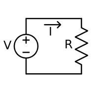
In this form the equation has no signal flow implied. It merely states that the resistance R is the voltage V divided by the current I. The resistor will obey Ohm’s law.
We can rearrange the equation as I = V / R
In this form, the equation states that the current is equal to the voltage divided by R. The circuit creates a current when a voltage is applied to the resistor. The voltage is the input and the current is the output.
We can also arrange the equation as V = I * R.
In this case, current creates a voltage. The current is the input and the voltage is the output.
Note that equations have signal flow from right to left. This is opposite to the schematic convention. Both conventions are well established. You need to remember the discrepancy. Sorry.
The Signal Flow convention for equations is the have the output on the right and the inputs on the left. The formula for a linear circuit is:
Output = ∑ k * Input
The equations can be retrieved from a SFG by summing the incoming branches. The above SFG has the following equations:
V1 = (Vin * g3) + (V2 * g1f) + (V3 * g5f)
V2 = (V1 * g1) + (V3 * g2f)
V3 = (V1 * g5) + (V2 * g2) + (Vout * g4f)
Vout = (V3 * g4)
The above equations are in the SFG format. This is not the General form for a system of Linear equations. The General form has a matrix structure.
|
V1 |
-g1f * V2 |
-g5f* V3 |
|
= g3 * Vin |
|
-g1 * V1 |
+ V2 |
-g2f * V3 |
|
= 0 |
|
-g5 * V1 |
-g2 * V2 |
+ V3 |
-g4f * Vout |
= 0 |
|
|
|
-g4 * V3 |
+ Vout |
= 0 |
In the General form there is
no Signal Flow implication. To create a SFG, you have to rearrange the
equations into the SFG format shown above. For each variable you select a
defining equation and put that equation into SFG form. There are many
ways to do this. Each selection set forms a SFG circuit description. Your
challenge is to pick a selection that matches your circuit operation intuition.
This is not always possible and you may create an ugly SFG.
Note that it is always possible to convert a SFG into a set of equations and vice versa. The circuit operation does not change. Circuits obey laws and don’t care what equations you used. The thing that changes is the signal flow description.
Circuit Description
Electronics provides a behavioral description for each circuit. This description is often copied and becomes the definitive description. Alternative descriptions are seldom mentioned; implying that that this description is the only valid description. Circuits have many different operating modes. Some are very sneaky. Some may be irrelevant. It is not possible to have a description that includes all modes of operation. Any description is only a partial description. Don’t place too much emphasis on the description. Any description is just one of many tales.
Another problem is that the concepts used in the descriptions vary widely from circuit to circuit. This makes Electronics confusing. There are simply too many different descriptions. The K9 VSA procedure creates a signal flow description from the schematic. The VSA SFG will show the signal flows selected by the VSA procedure. VSA makes all the choices. In this case, signals via the ground node are not shown. The K9 Ad Hoc procedure provides more freedom.
If you compare the Electronic description with the K9 description, you may find that the descriptions are totally different. It may not be possible to easily reconcile the differences. Don’t let this disturb you. Many valid descriptions are possible. You get to choose. Never insist that your interpretation is the only valid interpretation.
Try the VSA SFG description.
It’s easy, the procedure makes all the selections. If
you like the result, you may not have to write a lengthy circuit description. A
picture is worth a thousand words.
The SFG is discussed on the SFG page.