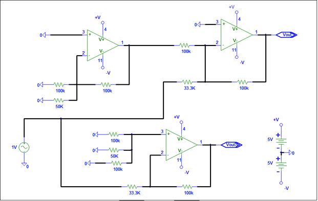
Two Op-amp Summing Circuit
A summing circuit with multiple positive and negative inputs can implement any linear circuit. The Legacy two op-amp circuit is shown below.
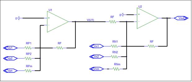
The circuit consists of a two Inverting Summing Amplifier circuits. U1 sums the positive gain inputs. U2 sums the negative gain inputs and inverts the output of U1.
On this page the circuit is transformed to a SFG and then compared with Shadow’s single op-amp implementation.
SFG Construction
Rather using an op-amp model as in the previous example. The circuit is modeled as two amplifiers.
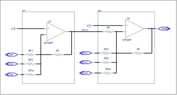
This is possible when all amplifier inputs are voltage controlled nodes. An amplifier has an input impedance that presents a load to the input. If the input has zero node impedance, then the amplifier load can not affect the input. There is no interaction between the input and the amplifier. Interaction between inputs is also not possible.
The SFG has a node for each circuit node. In this case the internal nodes of the amplifier are not modeled.
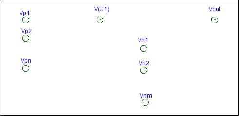
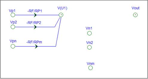
The SFG requires equations for V(U1) and Vout. The other nodes are inputs. The equation are obtained from Plato’s Gain formula. First check that the amplifier circuit is a General Summing amplifier. Next get the gain for each input. The SFG with the V(U1) equation is shown below.
Plato’s Gain formula requires ideal voltage inputs. In the case of U2, the V(U1) input is an op-amp output. Since the output impedance is zero, this qualifies as an ideal voltage input. The complete SFG is shown below.

A SFG node is a summing node that adds the signals from the incoming branches. In the above SFG a “+” has been added to the V(U1) and Vout node symbols for clarity. This is implied in SFGs. The normal SFG node symbol is a dot.
There are no loops in the SFG. The path gains are the actual circuit gains. Via Superposition ,
Vout = RF/RP1 * Vp1 + RF/RP2 *Vp2 + … + RF/RPm * Vpn
-RF/RN1 * Vn1 – RF/RN2 * Vn2 - … - RF/RNm * Vnm
The Vout equation can represent any linear circuit. This circuit can thus be used to implement any linear circuit. The same is true for the single op-amp General Amplifier circuit. Let’s compare them.
Linear Circuit design example
Design a linear circuit to implement
Vout = 1*V1 + 2* V2 – 3*V3
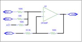
The circuit has two positive gain inputs and a negative gain input. In both cases the gain equation is Rf/Ri. Shadow added a ground resistor. The ground resistor is mandatory for the single op-amp design and optional for the two op-amp design.
|
Two op-amp |
Single op-amp |
|
|
|
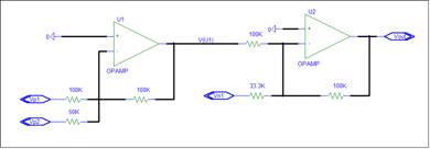
The two op-amp design uses an inverting gain circuit for each input. The inputs are independent. You can change any gain by simply changing the input resistor value. Changing the ground resistor is only needed for a balanced design; optional in many cases.
The Single op-amp circuit is more complicated. You can change any gain by simply changing the input resistor value, but the ground resistor value must be updated. This is not optional. Note that the location of the ground resistor may change. To be safe, when designing a circuit board, allow for a ground resistor on both op-amp inputs. Do not use both, just allow the ground resistor to be on either input.
The two op-amp solution has an extra op-amp and an additional resistor. If you need a balanced design, the two op-amp solution needs two more resistors. What do you get with the additional components?
The ideal response is the same for both circuits. Let’s analyze both circuits in more detail.
Bandwidth
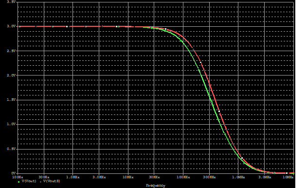
Let’s check the AC response of both circuits via simulation. First test the V1 input response. Unused inputs are connected to ground. The simulation uses the LM324/NS op-amp model. The schematic is shown below.
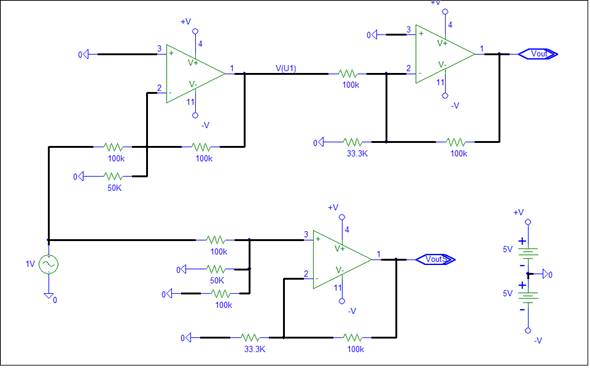
A 1 volt AC input is connected to the V1 input and the simulation output is shown below.
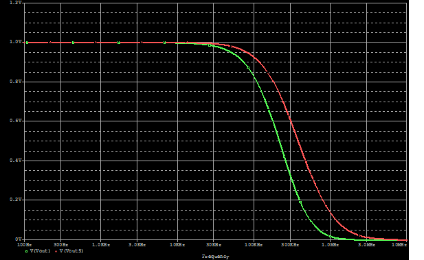
The single op-amp output is the red plot, while the dual op-amp output is the green plot. The single op-amp circuit has greater bandwidth for signals applied to the V1 input. Note that the V1 signal has to go thru two op-amps in the dual circuit. A reduction in bandwidth may be expected.
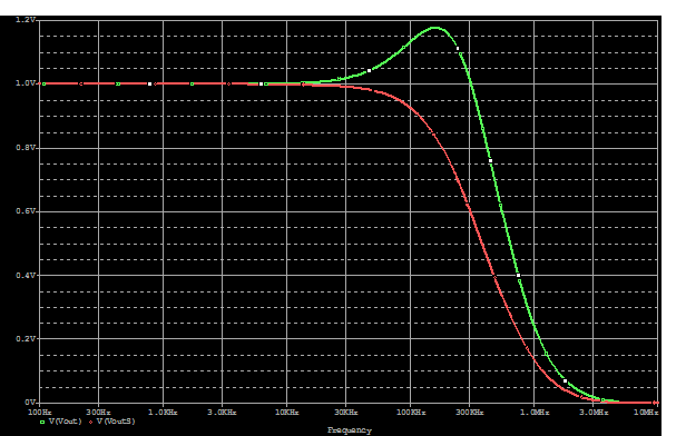
What about the V3 input? It goes thru a single op-amp in both cases.
In the above circuit the AC input is connected to the V3 inputs. The other inputs are grounded. The ground is needed to create the proper op-amp gain. The circuit will function on a bread board with an open negative input, but not provide precise results. The Simulator does not allow open connections. The simulation output is shown below.
In this case the magnitude of both gains is equal to three. The single op-amp circuit has greater bandwidth. Why ? Both circuits use a single op-amp. The op-amp bandwidth is determined by the net positive gain that the op-amp must deliver. The bandwidth is the Gain Bandwidth Product divided by the net positive gain.
In the dual op-amp circuit there are two negative gains, -3 and -1. The net positive gain is one more than the net negative gain (Daisy) and equal to +5. In the single op-amp circuit there is only one negative gain, -3. The net positive gain is +4.
Shadow’s single op-amp design has better bandwidth on all inputs. He designs the best circuit.
Ground Gain
Can the above gain argument be applied to Ground Gain? You want the ground gain to be a minimum to minimize ground noise in the output. The output op-amp in the dual solution has a negative gain of -4 and a ground gain of +5. The single op-amp circuit has a ground gain of +1. Does this make Shadow’s solution better?
If you consider only the output op-amp, Shadow’s solution appears to be much better, five times less noise. If you consider the entire circuit, there is no difference. Daisy says that the sum of gains is equal to one. This applies to entire circuits as well as sub-circuits. The ground gain for the dual op-amp circuit is the same as the single op-amp circuit, namely +1. This may be difficult to digest. So let’s test the conclusion via simulation. The Test Input is applied to all circuit and ground inputs.

The simulation output is shown below.
The ground gain magnitude is equal to one for low frequencies. When the op-amp gain rolls off, Shadow’s solution does have less ground gain, but not the large difference suggested by the output op-amp comparison.
Conclusion
Trust Shadow to Design the Best Circuit
For another example
of amplifier modeling look at the State
Variable Filter circuit.